Copper wiring
Wire interconnections within the package support the assembly of multiple components into a functional module.

Understand the components, assembly approaches and design considerations behind compact, functional semiconductor systems.
System-in-Package is an electronic system or subsystem integrated and miniaturized through IC assembly technologies. It can combine multiple chips and components with different functions within a single package or module.
Typical elements include specialised processors, DRAM, flash memory, resistors, capacitors, inductors, filters, connectors, MEMS devices, sensors and pre-assembled packages.
This heterogeneous integration requires consideration of the electrical system, component arrangement, interconnections, shielding, thermal behaviour and testing approach.
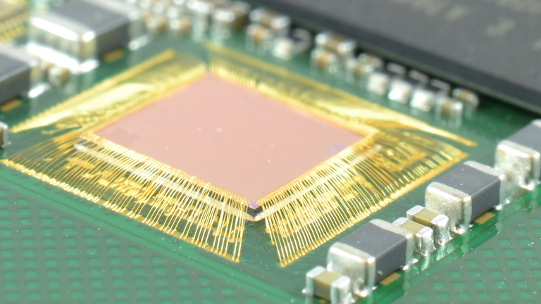
Wire interconnections within the package support the assembly of multiple components into a functional module.
Die-to-substrate interconnection is part of the assembly toolkit for compact, integrated devices.
Packaging at wafer level supports miniaturization across a range of electronic components.
Fan-out integration is one of the established assembly approaches used in advanced SiP development.
Multi-die and stacked structures introduce additional layout, interconnection and system-design considerations.
Embedded-die structures provide another route to integrate multiple functions within a compact package.
Surface-mount technology (SMT), encapsulation, shielding and interconnection assembly form part of the development approach.
Remote control, home automation, energy applications, connected devices and smart living.
The Wireless SiP module brings a 2.4 GHz BLE transceiver and ARM Cortex-M0 processor into a compact package.
Explore Wireless SiPNotebooks, tablets and compact computing products.
The Computing & Storage SiP module uses a double-sided structure with molded protection and NAND flash storage.
Explore Computing & Storage SiPIntegrated power devices, intelligent power switches and driver applications.
Embedded multi-die integration brings power devices, drivers and associated functions into a compact package. BI’s broader SiP solutions also address smart bikes and automotive applications.
Explore Power SiPPhysiological signal sensing, health and fitness devices, and optical sensing.
The Sensor & Optical SiP module combines LEDs and a photo-die with optical molding and an embedded-die substrate.
Explore Sensor & Optical SiPBI’s wider application focus includes smart cities, mobile and IoT devices, high-performance computing, artificial intelligence, 5G communication and AR/VR sensing. Discuss the requirements of your specific application with our team.
Share your application, package requirements and testing needs with our team.